What we've discovered
Read our papers here
No items found.

By leveraging their distinctive properties, we aim to develop materials that can transform technologies such as qunatum computing and spintronics.
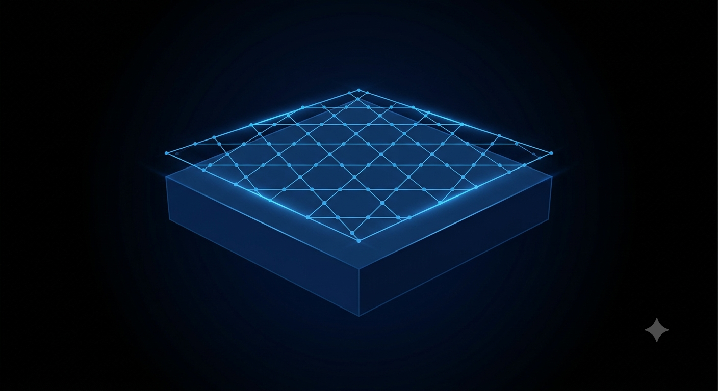
Using Molecular Beam Epitaxy (MBE) to deposit atoms layer-by-layer in ultra-high vaccuum (1e-10 mbar) to precisely fabricate atomically-thin layered materials.
RHEED and LEED for surface-sensitive diffraction measurements to determine crystal structure and geometry, performed in-situ.

Determine stoichiometric ratios using lab and synchrotron-based XPS, alongside exposure studies to analyse material composition and chemical stability.
.svg)
We characterise surface topography using AFM at the Melbourne Centre for Nanofabrication and measure surface roughness.

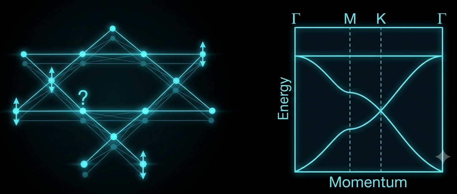
Using ARPES, we map electronic band structures to directly to reveal critical features such as flat bands and Dirac points.

Imaging nanoscale surface topology using STM and performing spectroscopy to directly probe the local density of states.